PHXII14:SEMICONDUCTOR ELECTRONICS- MATERIALS- DEVICES AND SIMPLE CIRCUITS
365232
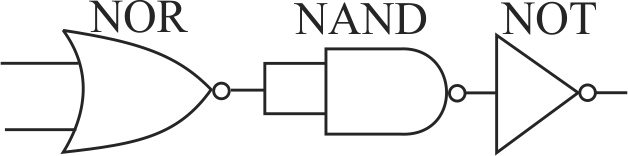
The circuit is equivalent to
1 AND gate
2 NAND gate
3 NOR gate
4 OR gate
Explanation:
The gate circuit can be solved by giving two inputs \(A\) and \(B\). Output of NOR gate, \({Y_1} = \overline {A + B} \) Output of NAND d gate,\({Y_2} = {\rm{ }}\overline {{Y_1} \cdot {Y_1}} = {Y_1}\) \( = \overline{\overline {{\rm{ }}A + B}} {\rm{ }} = {\rm{ }}A + B\) \(Y = \overline {{Y_2}} = \overline {A + B} \), which is of NOR gate
PHXII14:SEMICONDUCTOR ELECTRONICS- MATERIALS- DEVICES AND SIMPLE CIRCUITS
365233
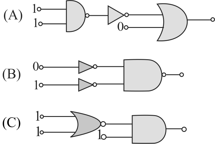
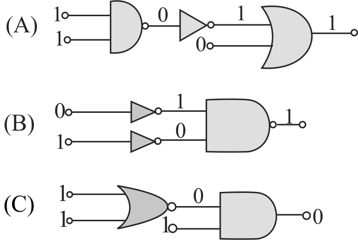
In the following combinations of logic gates, the outputs of \(A\), \(B\) and \(C\) are respectively
1 \(0,1,1\)
2 \(0,1,0\)
3 \(1,1,0\)
4 \(1,0,1\)
Explanation:
The outputs of \(A\), \(B\) and \(C\) are 1, 1, and 0 respectively.
KCET - 2009
PHXII14:SEMICONDUCTOR ELECTRONICS- MATERIALS- DEVICES AND SIMPLE CIRCUITS
365234
The output of a 2-input OR gate is zero only when its
1 Both inputs are 0
2 Either input is 1
3 Both inputs are 1
4 Either input is zero.
Explanation:
Conceptual Question
PHXII14:SEMICONDUCTOR ELECTRONICS- MATERIALS- DEVICES AND SIMPLE CIRCUITS
365235
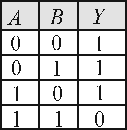
The truth table given below is for (\({A\,\& B}\) are the inputs and \(Y\) is the output)
1 NOR
2 AND
3 \(\mathrm{XOR}\)
4 NAND
Explanation:
The output \(Y = (\overline {A \cdot B} )\) is a combination of AND and NOT gates. Hence, the truth table is for NAND gate.
PHXII14:SEMICONDUCTOR ELECTRONICS- MATERIALS- DEVICES AND SIMPLE CIRCUITS
365236
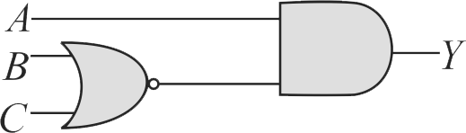
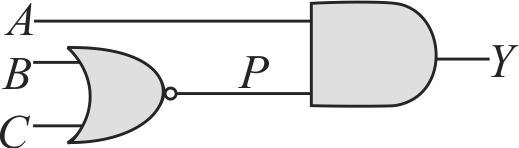
In the logic circuit diagram, \(A, B\) and \(C\) are the inputs, \(Y\) is the output. The output \(Y\) is 'HIGH'.
1 For all the inputs 'LOW'.
2 when \(A=1, B=0, C=0\)
3 when \(A=1, B=0, C=1\)
4 for all inputs 'HIGH'.
Explanation:
It is required that \(Y=1\) For this, both \(A\) and \(P\) shall be 1 as \(A\) and \(P\) are fed to \(A N D\) gate. we can take \(A=1\)But, in order that \(P\) to be 1 , which is output of \(N O R\) gate, neither of \(B\) and \(C\) shall be 1 \(\Rightarrow\) Both \(B\) and \(C\) shall be 0 \(\Rightarrow A=1, B=0, C=0\) will give \(Y=1\) So, correct option is (2)
PHXII14:SEMICONDUCTOR ELECTRONICS- MATERIALS- DEVICES AND SIMPLE CIRCUITS
365232
The circuit is equivalent to
1 AND gate
2 NAND gate
3 NOR gate
4 OR gate
Explanation:
The gate circuit can be solved by giving two inputs \(A\) and \(B\). Output of NOR gate, \({Y_1} = \overline {A + B} \) Output of NAND d gate,\({Y_2} = {\rm{ }}\overline {{Y_1} \cdot {Y_1}} = {Y_1}\) \( = \overline{\overline {{\rm{ }}A + B}} {\rm{ }} = {\rm{ }}A + B\) \(Y = \overline {{Y_2}} = \overline {A + B} \), which is of NOR gate
PHXII14:SEMICONDUCTOR ELECTRONICS- MATERIALS- DEVICES AND SIMPLE CIRCUITS
365233
In the following combinations of logic gates, the outputs of \(A\), \(B\) and \(C\) are respectively
1 \(0,1,1\)
2 \(0,1,0\)
3 \(1,1,0\)
4 \(1,0,1\)
Explanation:
The outputs of \(A\), \(B\) and \(C\) are 1, 1, and 0 respectively.
KCET - 2009
PHXII14:SEMICONDUCTOR ELECTRONICS- MATERIALS- DEVICES AND SIMPLE CIRCUITS
365234
The output of a 2-input OR gate is zero only when its
1 Both inputs are 0
2 Either input is 1
3 Both inputs are 1
4 Either input is zero.
Explanation:
Conceptual Question
PHXII14:SEMICONDUCTOR ELECTRONICS- MATERIALS- DEVICES AND SIMPLE CIRCUITS
365235
The truth table given below is for (\({A\,\& B}\) are the inputs and \(Y\) is the output)
1 NOR
2 AND
3 \(\mathrm{XOR}\)
4 NAND
Explanation:
The output \(Y = (\overline {A \cdot B} )\) is a combination of AND and NOT gates. Hence, the truth table is for NAND gate.
PHXII14:SEMICONDUCTOR ELECTRONICS- MATERIALS- DEVICES AND SIMPLE CIRCUITS
365236
In the logic circuit diagram, \(A, B\) and \(C\) are the inputs, \(Y\) is the output. The output \(Y\) is 'HIGH'.
1 For all the inputs 'LOW'.
2 when \(A=1, B=0, C=0\)
3 when \(A=1, B=0, C=1\)
4 for all inputs 'HIGH'.
Explanation:
It is required that \(Y=1\) For this, both \(A\) and \(P\) shall be 1 as \(A\) and \(P\) are fed to \(A N D\) gate. we can take \(A=1\)But, in order that \(P\) to be 1 , which is output of \(N O R\) gate, neither of \(B\) and \(C\) shall be 1 \(\Rightarrow\) Both \(B\) and \(C\) shall be 0 \(\Rightarrow A=1, B=0, C=0\) will give \(Y=1\) So, correct option is (2)