PHXII14:SEMICONDUCTOR ELECTRONICS- MATERIALS- DEVICES AND SIMPLE CIRCUITS
365237
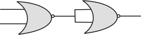
Identify the logic operation performed by the circuit given here
1 OR
2 NOR
3 NOT
4 NAND
Explanation:
\(Y = \overline {\overline {A + B} } = A + B\) It is the Boolean expression of OR gate
KCET - 2010
PHXII14:SEMICONDUCTOR ELECTRONICS- MATERIALS- DEVICES AND SIMPLE CIRCUITS
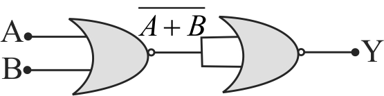
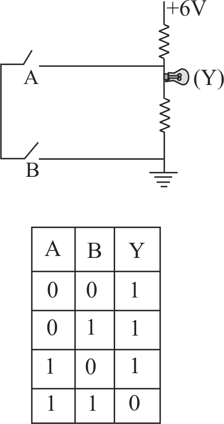
365238
The correct Boolean operation represented by the circuit diagram drawn is :
1 AND
2 OR
3 NAND
4 NOR
Explanation:
When two switches are closed then current does not pass through the bulb Truth Table This is output of NAND gate.
NEET - 2019
PHXII14:SEMICONDUCTOR ELECTRONICS- MATERIALS- DEVICES AND SIMPLE CIRCUITS
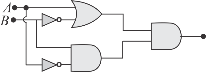
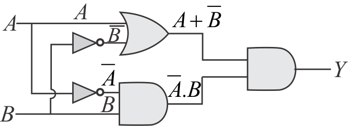
365239
The output \(Y\) of following circuit for given input is
1 \(A \cdot B\)
2 0
3 \(A \cdot B(A+B)\)
4 \(\bar{A} \cdot B\)
Explanation:
\(Y=(A+\bar{B}) \cdot(\bar{A} \cdot B)=A \cdot \bar{A} \cdot B+\bar{B} \cdot \bar{A} \cdot B=0\) \([\because A \cdot \bar{A}=0\) and \(B \cdot \bar{B}=0]\)
JEE - 2024
PHXII14:SEMICONDUCTOR ELECTRONICS- MATERIALS- DEVICES AND SIMPLE CIRCUITS
365240
Assertion : NOT gate is also called inverter circuit. Reason : NOT gate inverts the input logic.
1 Both Assertion and Reason are correct and Reason is the correct explanation of the Assertion.
2 Both Assertion and Reason are correct but Reason is not the correct explanation of the Assertion.
3 Assertion is correct but Reason is incorrect.
4 Assertion is incorrect but reason is correct.
Explanation:
Symbol of NOT : The NOT gate, or inverter, inversely outputs \((Y)\) a low (0) for a high (1) input \((A)\) and vice versa. Named for its logic inversion, it is a fundamental element in digital circuits for logical negation. So correct option is (1).
PHXII14:SEMICONDUCTOR ELECTRONICS- MATERIALS- DEVICES AND SIMPLE CIRCUITS
365237
Identify the logic operation performed by the circuit given here
1 OR
2 NOR
3 NOT
4 NAND
Explanation:
\(Y = \overline {\overline {A + B} } = A + B\) It is the Boolean expression of OR gate
KCET - 2010
PHXII14:SEMICONDUCTOR ELECTRONICS- MATERIALS- DEVICES AND SIMPLE CIRCUITS
365238
The correct Boolean operation represented by the circuit diagram drawn is :
1 AND
2 OR
3 NAND
4 NOR
Explanation:
When two switches are closed then current does not pass through the bulb Truth Table This is output of NAND gate.
NEET - 2019
PHXII14:SEMICONDUCTOR ELECTRONICS- MATERIALS- DEVICES AND SIMPLE CIRCUITS
365239
The output \(Y\) of following circuit for given input is
1 \(A \cdot B\)
2 0
3 \(A \cdot B(A+B)\)
4 \(\bar{A} \cdot B\)
Explanation:
\(Y=(A+\bar{B}) \cdot(\bar{A} \cdot B)=A \cdot \bar{A} \cdot B+\bar{B} \cdot \bar{A} \cdot B=0\) \([\because A \cdot \bar{A}=0\) and \(B \cdot \bar{B}=0]\)
JEE - 2024
PHXII14:SEMICONDUCTOR ELECTRONICS- MATERIALS- DEVICES AND SIMPLE CIRCUITS
365240
Assertion : NOT gate is also called inverter circuit. Reason : NOT gate inverts the input logic.
1 Both Assertion and Reason are correct and Reason is the correct explanation of the Assertion.
2 Both Assertion and Reason are correct but Reason is not the correct explanation of the Assertion.
3 Assertion is correct but Reason is incorrect.
4 Assertion is incorrect but reason is correct.
Explanation:
Symbol of NOT : The NOT gate, or inverter, inversely outputs \((Y)\) a low (0) for a high (1) input \((A)\) and vice versa. Named for its logic inversion, it is a fundamental element in digital circuits for logical negation. So correct option is (1).