PHXII14:SEMICONDUCTOR ELECTRONICS- MATERIALS- DEVICES AND SIMPLE CIRCUITS
365228
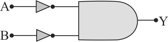
The output \(Y\) of the gate circuit shown in the figure below is
1 \(\overline {A.B} \)
2 \(\overline A .\overline B \)
3 \(\overline{\overline {A.B}} \)
4 \(\overline A \, + \,\overline B \)
Explanation:
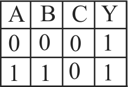
The input of AND gate is \({\bar A}\) and \(\bar B \Rightarrow Y = \bar A.\bar B\)
PHXII14:SEMICONDUCTOR ELECTRONICS- MATERIALS- DEVICES AND SIMPLE CIRCUITS
365229
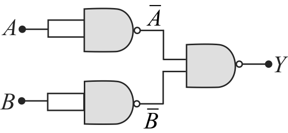
To get an OR gate from a NAND gate, we need
1 only two NAND gates.
2 two NOT gates obtained from NAND gates and one NAND gate.
3 four NAND gates and two AND gates obtained from NAND gates.
4 none of these
Explanation:
To obtain an OR gate from NAND gates, we need two NOT gates obtained from NAND gates and one NAND gate as shown in figure.
The Boolean expression is \(Y=\overline{\bar{A} \cdot \bar{B}}=\overline{\bar{A}}+\overline{\bar{B}}\)\(\,\,\,\,\)(by De Morgan's theorem) \(=A+B\)\(\,\,\,\,\)\((\because \overline{\bar{A}}=A \text { and } \overline{\bar{B}}=B)\) It is same as of \(OR\) gate.
PHXII14:SEMICONDUCTOR ELECTRONICS- MATERIALS- DEVICES AND SIMPLE CIRCUITS
365230
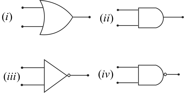
Symbolic representation of four logic gates are shown as Pick out which ones are for AND, NAND and NOT gates, respectively.
1 (\(iii\)), (\(ii\)) and (\(i\))
2 (\(iii\)), (\(ii\)) and (\(iv\))
3 (\(ii\)), (\(iv\)) and (\(iii\))
4 (\(ii\)), (\(iii\)) and (\(iv\))
Explanation:
The symbols given in problems are (i) OR (ii) AND (iii) NOT (iv) NAND
PHXII14:SEMICONDUCTOR ELECTRONICS- MATERIALS- DEVICES AND SIMPLE CIRCUITS
365231
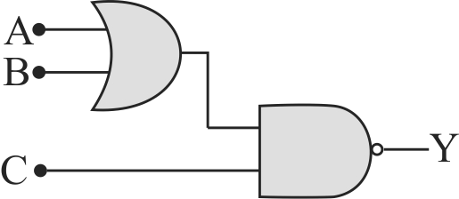
For the given combination of gates, if the logic states of inputs \(A,B,C\) are as follows \(A = B = C = 0\) and \(A = B = 1,C = 0\) then the logic states of output \(D\) are
NEET Test Series from KOTA - 10 Papers In MS WORD
WhatsApp Here
PHXII14:SEMICONDUCTOR ELECTRONICS- MATERIALS- DEVICES AND SIMPLE CIRCUITS
365228
The output \(Y\) of the gate circuit shown in the figure below is
1 \(\overline {A.B} \)
2 \(\overline A .\overline B \)
3 \(\overline{\overline {A.B}} \)
4 \(\overline A \, + \,\overline B \)
Explanation:
The input of AND gate is \({\bar A}\) and \(\bar B \Rightarrow Y = \bar A.\bar B\)
PHXII14:SEMICONDUCTOR ELECTRONICS- MATERIALS- DEVICES AND SIMPLE CIRCUITS
365229
To get an OR gate from a NAND gate, we need
1 only two NAND gates.
2 two NOT gates obtained from NAND gates and one NAND gate.
3 four NAND gates and two AND gates obtained from NAND gates.
4 none of these
Explanation:
To obtain an OR gate from NAND gates, we need two NOT gates obtained from NAND gates and one NAND gate as shown in figure.
The Boolean expression is \(Y=\overline{\bar{A} \cdot \bar{B}}=\overline{\bar{A}}+\overline{\bar{B}}\)\(\,\,\,\,\)(by De Morgan's theorem) \(=A+B\)\(\,\,\,\,\)\((\because \overline{\bar{A}}=A \text { and } \overline{\bar{B}}=B)\) It is same as of \(OR\) gate.
PHXII14:SEMICONDUCTOR ELECTRONICS- MATERIALS- DEVICES AND SIMPLE CIRCUITS
365230
Symbolic representation of four logic gates are shown as Pick out which ones are for AND, NAND and NOT gates, respectively.
1 (\(iii\)), (\(ii\)) and (\(i\))
2 (\(iii\)), (\(ii\)) and (\(iv\))
3 (\(ii\)), (\(iv\)) and (\(iii\))
4 (\(ii\)), (\(iii\)) and (\(iv\))
Explanation:
The symbols given in problems are (i) OR (ii) AND (iii) NOT (iv) NAND
PHXII14:SEMICONDUCTOR ELECTRONICS- MATERIALS- DEVICES AND SIMPLE CIRCUITS
365231
For the given combination of gates, if the logic states of inputs \(A,B,C\) are as follows \(A = B = C = 0\) and \(A = B = 1,C = 0\) then the logic states of output \(D\) are
PHXII14:SEMICONDUCTOR ELECTRONICS- MATERIALS- DEVICES AND SIMPLE CIRCUITS
365228
The output \(Y\) of the gate circuit shown in the figure below is
1 \(\overline {A.B} \)
2 \(\overline A .\overline B \)
3 \(\overline{\overline {A.B}} \)
4 \(\overline A \, + \,\overline B \)
Explanation:
The input of AND gate is \({\bar A}\) and \(\bar B \Rightarrow Y = \bar A.\bar B\)
PHXII14:SEMICONDUCTOR ELECTRONICS- MATERIALS- DEVICES AND SIMPLE CIRCUITS
365229
To get an OR gate from a NAND gate, we need
1 only two NAND gates.
2 two NOT gates obtained from NAND gates and one NAND gate.
3 four NAND gates and two AND gates obtained from NAND gates.
4 none of these
Explanation:
To obtain an OR gate from NAND gates, we need two NOT gates obtained from NAND gates and one NAND gate as shown in figure.
The Boolean expression is \(Y=\overline{\bar{A} \cdot \bar{B}}=\overline{\bar{A}}+\overline{\bar{B}}\)\(\,\,\,\,\)(by De Morgan's theorem) \(=A+B\)\(\,\,\,\,\)\((\because \overline{\bar{A}}=A \text { and } \overline{\bar{B}}=B)\) It is same as of \(OR\) gate.
PHXII14:SEMICONDUCTOR ELECTRONICS- MATERIALS- DEVICES AND SIMPLE CIRCUITS
365230
Symbolic representation of four logic gates are shown as Pick out which ones are for AND, NAND and NOT gates, respectively.
1 (\(iii\)), (\(ii\)) and (\(i\))
2 (\(iii\)), (\(ii\)) and (\(iv\))
3 (\(ii\)), (\(iv\)) and (\(iii\))
4 (\(ii\)), (\(iii\)) and (\(iv\))
Explanation:
The symbols given in problems are (i) OR (ii) AND (iii) NOT (iv) NAND
PHXII14:SEMICONDUCTOR ELECTRONICS- MATERIALS- DEVICES AND SIMPLE CIRCUITS
365231
For the given combination of gates, if the logic states of inputs \(A,B,C\) are as follows \(A = B = C = 0\) and \(A = B = 1,C = 0\) then the logic states of output \(D\) are