
365495
A common emitter amplifier circuit, built using an n-p-n transistor, is shown in the figure. Its \(DC\) current gain is \(250, {R}_{{C}}=5 \,{k} \Omega\) and \({V}_{{CC}}=10 {~V}\). What is the minimum base current for \({V}_{{CE}}\) to reach saturation?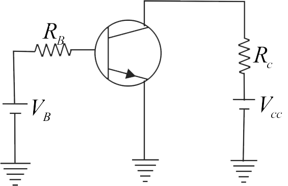
365497 A \(npn\) transistor is connected in common emitter configuration in a given amplifier. A load resistance of \(800\Omega \) is connected in the collector circuit and the voltage drop across it is 0.8 \(V\). If the current amplification factor is 0.96 and the input resistance of the circuit is \(192\Omega \), the voltage gain and the power gain of the amplifier will respectively be:
365498
Assertion :
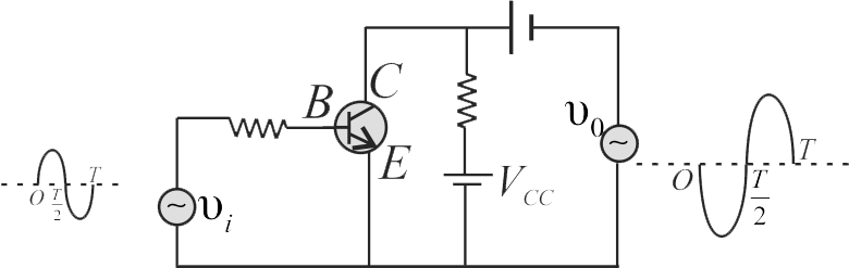
In a transistor amplifier (in common emitter configuration), the output voltage is always out of phase with the input voltage.
Reason :
The emitter base junction is reverse biased and the base collector junction is forward biased.
365495
A common emitter amplifier circuit, built using an n-p-n transistor, is shown in the figure. Its \(DC\) current gain is \(250, {R}_{{C}}=5 \,{k} \Omega\) and \({V}_{{CC}}=10 {~V}\). What is the minimum base current for \({V}_{{CE}}\) to reach saturation?
365497 A \(npn\) transistor is connected in common emitter configuration in a given amplifier. A load resistance of \(800\Omega \) is connected in the collector circuit and the voltage drop across it is 0.8 \(V\). If the current amplification factor is 0.96 and the input resistance of the circuit is \(192\Omega \), the voltage gain and the power gain of the amplifier will respectively be:
365498
Assertion :
In a transistor amplifier (in common emitter configuration), the output voltage is always out of phase with the input voltage.
Reason :
The emitter base junction is reverse biased and the base collector junction is forward biased.