PHXII14:SEMICONDUCTOR ELECTRONICS- MATERIALS- DEVICES AND SIMPLE CIRCUITS
365333
The width of the depletion region in a \(P\) - \(N\) junction diode is
1 Increased by reverse bias
2 Increased by forward bias
3 Decreased by reverse bias
4 Independent of the bias voltage
Explanation:
The width of the depletion region in a \(P\) - \(N\) junction diode is increased by reverse bias and decreased by forward bias
PHXII14:SEMICONDUCTOR ELECTRONICS- MATERIALS- DEVICES AND SIMPLE CIRCUITS
365334
In forward bias, the width of depletion layer is
1 decreases with decrease in potential barrier voltage
2 increases with increase in potential barrier voltage
3 independent of potential barrier voltage
4 None of the above
Explanation:
In forward biasing, the forward bias voltage opposes the potential barrier \({V_B}\). Due to it, the potential barrier is considerably reduced and the depletion region becomes thin. The potential barrier at some forward voltage \(\left( {0.1\,{\mkern 1mu} {\text{to}}\,{\mkern 1mu} 0.3\,V} \right)\), is eliminated altogether.
PHXII14:SEMICONDUCTOR ELECTRONICS- MATERIALS- DEVICES AND SIMPLE CIRCUITS
365335
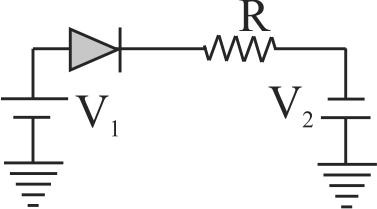
If \({V_1} > {V_2},r\) is resistance offered by diode in forward bias then current through the diode is
PHXII14:SEMICONDUCTOR ELECTRONICS- MATERIALS- DEVICES AND SIMPLE CIRCUITS
365333
The width of the depletion region in a \(P\) - \(N\) junction diode is
1 Increased by reverse bias
2 Increased by forward bias
3 Decreased by reverse bias
4 Independent of the bias voltage
Explanation:
The width of the depletion region in a \(P\) - \(N\) junction diode is increased by reverse bias and decreased by forward bias
PHXII14:SEMICONDUCTOR ELECTRONICS- MATERIALS- DEVICES AND SIMPLE CIRCUITS
365334
In forward bias, the width of depletion layer is
1 decreases with decrease in potential barrier voltage
2 increases with increase in potential barrier voltage
3 independent of potential barrier voltage
4 None of the above
Explanation:
In forward biasing, the forward bias voltage opposes the potential barrier \({V_B}\). Due to it, the potential barrier is considerably reduced and the depletion region becomes thin. The potential barrier at some forward voltage \(\left( {0.1\,{\mkern 1mu} {\text{to}}\,{\mkern 1mu} 0.3\,V} \right)\), is eliminated altogether.
PHXII14:SEMICONDUCTOR ELECTRONICS- MATERIALS- DEVICES AND SIMPLE CIRCUITS
365335
If \({V_1} > {V_2},r\) is resistance offered by diode in forward bias then current through the diode is
NEET Test Series from KOTA - 10 Papers In MS WORD
WhatsApp Here
PHXII14:SEMICONDUCTOR ELECTRONICS- MATERIALS- DEVICES AND SIMPLE CIRCUITS
365333
The width of the depletion region in a \(P\) - \(N\) junction diode is
1 Increased by reverse bias
2 Increased by forward bias
3 Decreased by reverse bias
4 Independent of the bias voltage
Explanation:
The width of the depletion region in a \(P\) - \(N\) junction diode is increased by reverse bias and decreased by forward bias
PHXII14:SEMICONDUCTOR ELECTRONICS- MATERIALS- DEVICES AND SIMPLE CIRCUITS
365334
In forward bias, the width of depletion layer is
1 decreases with decrease in potential barrier voltage
2 increases with increase in potential barrier voltage
3 independent of potential barrier voltage
4 None of the above
Explanation:
In forward biasing, the forward bias voltage opposes the potential barrier \({V_B}\). Due to it, the potential barrier is considerably reduced and the depletion region becomes thin. The potential barrier at some forward voltage \(\left( {0.1\,{\mkern 1mu} {\text{to}}\,{\mkern 1mu} 0.3\,V} \right)\), is eliminated altogether.
PHXII14:SEMICONDUCTOR ELECTRONICS- MATERIALS- DEVICES AND SIMPLE CIRCUITS
365335
If \({V_1} > {V_2},r\) is resistance offered by diode in forward bias then current through the diode is
PHXII14:SEMICONDUCTOR ELECTRONICS- MATERIALS- DEVICES AND SIMPLE CIRCUITS
365333
The width of the depletion region in a \(P\) - \(N\) junction diode is
1 Increased by reverse bias
2 Increased by forward bias
3 Decreased by reverse bias
4 Independent of the bias voltage
Explanation:
The width of the depletion region in a \(P\) - \(N\) junction diode is increased by reverse bias and decreased by forward bias
PHXII14:SEMICONDUCTOR ELECTRONICS- MATERIALS- DEVICES AND SIMPLE CIRCUITS
365334
In forward bias, the width of depletion layer is
1 decreases with decrease in potential barrier voltage
2 increases with increase in potential barrier voltage
3 independent of potential barrier voltage
4 None of the above
Explanation:
In forward biasing, the forward bias voltage opposes the potential barrier \({V_B}\). Due to it, the potential barrier is considerably reduced and the depletion region becomes thin. The potential barrier at some forward voltage \(\left( {0.1\,{\mkern 1mu} {\text{to}}\,{\mkern 1mu} 0.3\,V} \right)\), is eliminated altogether.
PHXII14:SEMICONDUCTOR ELECTRONICS- MATERIALS- DEVICES AND SIMPLE CIRCUITS
365335
If \({V_1} > {V_2},r\) is resistance offered by diode in forward bias then current through the diode is