365359
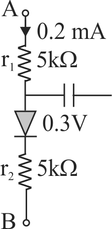
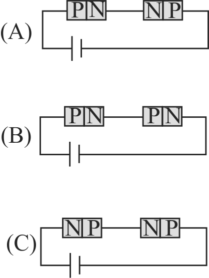
In the circuit below, \(A\) and \(B\) represent two inputs and \({C}\) represents the output.
The circuit represents a logic gate for which, values of \(A,B\) and \(C\) are as follows:
Determine the value of \(x\). (Consider all the compound in the circuit to be ideal.)
365359
In the circuit below, \(A\) and \(B\) represent two inputs and \({C}\) represents the output.
The circuit represents a logic gate for which, values of \(A,B\) and \(C\) are as follows:
Determine the value of \(x\). (Consider all the compound in the circuit to be ideal.)
365359
In the circuit below, \(A\) and \(B\) represent two inputs and \({C}\) represents the output.
The circuit represents a logic gate for which, values of \(A,B\) and \(C\) are as follows:
Determine the value of \(x\). (Consider all the compound in the circuit to be ideal.)
365359
In the circuit below, \(A\) and \(B\) represent two inputs and \({C}\) represents the output.
The circuit represents a logic gate for which, values of \(A,B\) and \(C\) are as follows:
Determine the value of \(x\). (Consider all the compound in the circuit to be ideal.)
365359
In the circuit below, \(A\) and \(B\) represent two inputs and \({C}\) represents the output.
The circuit represents a logic gate for which, values of \(A,B\) and \(C\) are as follows:
Determine the value of \(x\). (Consider all the compound in the circuit to be ideal.)